No.3328
Global Wide-Bandgap Monocrystalline Semiconductor Material Market: Key Research Findings 2023
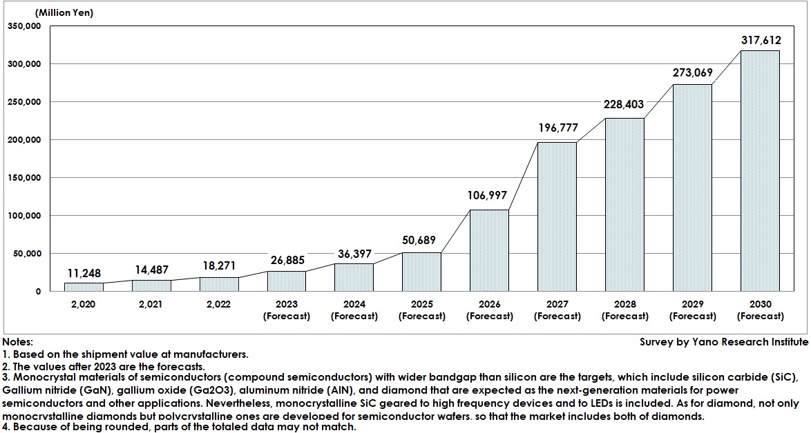
Global Wide-Bandgap Monocrystalline Semiconductor Material Market Expected to Reach 317,600 Million Yen by 2030
Yano Research Institute (the President, Takashi Mizukoshi) carried out a survey on the global wide-bandgap monocrystalline semiconductor material market, and found out the trends by product segment, the trends of market players, and the future perspectives.
Market Overview
The market of wide bandgap monocrystalline semiconductor materials is expanding year by year, as their main applications to power semiconductor devices as a replacement of silicon are expanding. The global market size by shipment value at manufacturers in 2022 has been estimated as 18,271 million yen, and for 2023 it is estimated to reach 26,885 million yen.
When observing the market size estimation by material for 2023, silicon carbide (SiC) dominates 75.5% of the market at 20,293 million yen, Gallium nitride (GaN) occupies 17.3% at 4,647 million yen, gallium oxide (Ga2O3) accounts for 2.0% at 531 million yen, Aluminum nitride (AlN) accounts for 4.0% at 1,080 million yen, and diamond occupies 1.2% at 335 million yen, showing that SiC is estimated to occupy three fourth of the market.
The market trends by material are as follows:
SiC is approaching at a full-fledged growth stage, as it is likely to burgeon for automotive applications after 2025.
GaN is currently applied for lighing such as light-emitting diodes (LEDs) and laser diodes (LDs), but its outstanding characteristics when used for power devices and high frequencies, and a sign of improvements in its challenges of creating larger-diameter wafers and mass supplies, causing it to be about to be developed as GaN-on-GaN devices.
Ga2O3, with its higher potential in cost and performance than SiC devices, is increasing the market players dealing in it. Because of fruitful outcomes announced one after another that make up for short period of research and development, it is promising material despite being a late comer.
Added with the impact of corona crisis, AlN has acquired a certain level of demand as a monocrystalline material geared for deep ultraviolet (UV) light-emitting diodes (LEDs). However, improvement in the performance of sapphire-substrate used LEDs for deep UV, AlN has a challenge of finding best applications for it to exert its strength.
Diamond has a sign of burgeoning. Domestic monocrystalline material manufacturers are increasing their production capacity by fund procurement through IPO, while universities and other R&D institutions have developed world's highest performance devices.
Noteworthy Topics
[Diamond]: Faster Development Speed for Materials and Devices due to Wafer Manufacturers' IPO and Increased Joint Study Results
As of 2023, Orbray is about to start supplying 2-inch diamond wafers. Ookuma Diamond Device is also preparing for mass production of diamond-used electronic devices.
In order for diamond, with its splendid properties, to expand the market as a new generation semiconductor component wafer, it is required to be embedded in devices with extremely high value-added demand no matter how niche. This is because the devices are something that can only be realized by diamond, making them very useful and specially positioned as universal, despite the scale of use may be small.
Future Outlook
Due to expansion in power-device applications, the global wide bandgap monocrystalline material market is expected to expand furthermore to 317,612 million yen by 2030 based on shipment value at manufacturers. When observing this by material, SiC is expected to grow to 307,348 million yen, GaN to 5,280 million yen, Ga2O3 3,056 million yen, AlN 1,350 million yen, and diamond 5,178 million yen. As can see, SiC is projected to occupy 96.8% of the market, quite marked difference than other materials in the status of mass production and the spreading period.
For SiC, 6-inch wafers are dominant, while the launch of 8-inch wafers seems to be close at hand. The number of alliances and related companies, including upstream and downstream commercial distribution companies, is increasing. The competition between wide bandgap monocrystalline materials is becoming fiercer, and the future of new materials is to be determined by the competitions over performance and cost.
Research Outline
2.Research Object: Manufacturers of wide-bandgap monocrystalline semiconductor materials, related companies, research institutions, etc.
3.Research Methogology: Face-to-face and online interviews by expert researchers
About Wide-Bandgap Monocrystalline Semiconductor Materials
Wide-bandgap monocrystalline semiconductor materials in this research refer to monocrystal materials of semiconductors (compound semiconductors) with wider bandgap than silicon, which include silicon carbide (SiC), Gallium nitride (GaN), gallium oxide (Ga2O3), aluminum nitride (AlN), and diamond that are expected as the next-generation materials for power semiconductors and other applications.
Nevertheless, monocrystalline SiC geared to high frequency devices and to LEDs is not included.
As for diamond, not only monocrystalline diamonds but polycrystalline ones are developed for semiconductor wafers, so that the market includes both of diamonds.
<Products and Services in the Market>
Wide bandgap monocrystalline semiconductor wafer
Published Report
Contact Us
The copyright and all other rights pertaining to this report belong to Yano Research Institute.
Please contact our PR team when quoting the report contents for the purpose other than media coverage.
Depending on the purpose of using our report, we may ask you to present your sentences for confirmation beforehand.