No.3929
Global Wide-Bandgap Semiconductor Single Crystal Market: Key Research Findings 2025
Slowdown in Growth of BEVs and Other Eco-Friendly Vehicles and Decreased Demand for Disinfections Affecting Material Growth
Yano Research Institute (the President, Takashi Mizukoshi) conducted a survey of the global wide-bandgap semiconductor single crystal market. The survey revealed the market size by ingredient, trend of products, technologies, and market players.
Market Overview
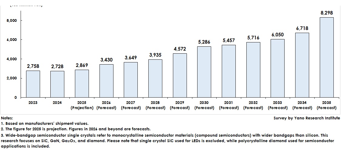
Based on manufacturers’ shipment values, the global wide-bandgap semiconductor single-crystal market— comprising silicon carbide (SiC), gallium nitride (GaN), gallium oxide (Ga₂O₃), and diamond— is projected to reach 286.9 billion yen in 2025.
Wide-bandgap semiconductor single crystals are primarily adopted for power semiconductor applications, which are increasingly used in battery electric vehicles (BEVs), railway vehicles, industrial equipment, renewable energy facilities, and datacenters. While SiC and GaN are already in use as devices in end products (applications), Ga₂O₃, and diamond remain in the research and development phase. Therefore, the development stage varies by material.
The current statuses by material are as follows:
SiC is leading the market, with adoption expanding mainly in automotive applications. Toward 2030, wafer suppliers are moving forward with plans to increase production; however, the growth of BEVs and other eco-friendly vehicles is slowing.
GaN ranks second among wide-bandgap semiconductors. Its main applications are light-emitting diodes (LEDs) and laser diodes (LDs). However, efforts are underway to increase wafer diameters to support high-frequency and power device applications. Mass production of four-inch wafers is imminent.
Ga₂O₃, a promising next-generation material, is showing signs of rapid growth. Six-inch wafer mass production is planned by 2026, driven by an increasing number of wafer suppliers. A consortium established in Japan aims to standardize Ga₂O₃ and promote its application expansion.
Diamond, considered the ultimate semiconductor material, is also exhibiting rapid progress. The number of wafer suppliers and device manufacturers is increasing, particularly among university-affiliated venture companies. Japan currently leads global research and development in diamond semiconductors.
Although aluminum nitride (AlN) is not included in this research, demand for its use in disinfection applications has declined since the end of the pandemic. However, the development of AlN heterojunctions with other semiconductor materials is underway, as these materials can be used to create high-performance devices for laser and high-frequency applications.
Rutile-type germanium dioxide (r-GeO₂) is expected to offer superior performance and better cost efficiency compared to other materials. Theoretically, r-GeO₂ can exhibit both p-type and n-type conductivity, which has made it a notable new material for power devices in recent years.
Noteworthy Topics
Increase in SiC Wafer Manufacturing Using Solution Growth Method, Projected Market Entry
SiC single crystal wafers are manufactured from powdered SiC using various methods. The process involves SiC passing through liquid and vapor phases before crystal growth occurs. After growth, the material forms a silicon carbide boule (ingot), which is then sliced and polished into wafers.
Although wafer manufacturing methods vary by company, the sublimation and solution growth methods are the most common approaches. While many companies have traditionally used the sublimation method, a growing number have adopted the solution growth method in recent years. Sublimation is the conventional technique for growing SiC single crystals, and most commercially available SiC single crystal wafers are currently produced using this process. However, because it involves heating and sublimating the solid (powder) state, thermal distortion can occur if the temperature gradient within the crystal is not properly controlled. Such distortion hinders the production of larger-diameter wafers and leads to crystal defects.
In contrast, the solution growth method does not produce a temperature gradient within the crystal, thereby limiting thermal distortion. In principle, this limitation makes it easier to produce larger-diameter wafers with fewer defects. Additionally, the solution growth method is faster, more cost-efficient, and has greater length adequacy. However, many companies have challenged this method in the past and abandoned it. The reason was that there were too many parameters to manage during crystal growth, and the optimal growth conditions could not be determined.
After overcoming these challenges, several wafer manufacturers are now adopting the solution growth method and are preparing for market introduction. In Japan, Central Glass and Oxide Power Crystal are leading the way, and several Chinese companies are also considering adopting the process. To date, there have been no confirmed attempts to use this method in Europe or the United States.
Unlike wafers produced by the sublimation method, which are limited to n-type and semi-insulating types, SiC wafers produced by the solution growth method can support p-type semiconductors and can expand applications to new structures. Consequently, despite the method's challenges, an increasing number of companies are expected to adopt it, because it contributes to advancements in SiC power devices.
Future Outlook
The global market for wide bandgap semiconductor single crystals is projected to increase adoption and installations in end products and applications after demands increase in the R&D fields. Although the growth rate varies by material, the global wide bandgap semiconductor single crystal market which comprises SiC, GaN, Ga₂O₃, and diamond, is projected to reach 829.8 billion yen by 2035.
As for SiC single crystal wafers, which precede other single crystal materials, 6-inch wafers currently dominate the market, though 8-inch wafers are gaining ground. Chinese suppliers are expanding their production capacity and increasing their market presence. Looking ahead, fierce competition is expected in the wide bandgap semiconductor single crystal market. The future of new materials depends on how this competition plays out in terms of performance and cost.
Research Outline
2.Research Object: Manufacturers of wide-bandgap semiconductor single crystals, related device manufacturers, research institutions, etc.
3.Research Methogology: Face-to-face and online interviews by expert researchers
About the Wide-Bandgap Semiconductor Single Crystal Market
Wide-bandgap semiconductor single crystals refer to monocrystalline semiconductor materials (compound semiconductors) with wider bandgaps than silicon. These include silicon carbide (SiC), gallium nitride (GaN), gallium oxide (Ga₂O₃), diamond, aluminum nitride (AlN), and germanium dioxide (GeO₂).
This research on the wide-bandgap semiconductor single crystal market focuses on four materials: SiC, GaN, Ga₂O₃, and diamond. Market size is based on manufacturers’ shipment values. Please note that single crystal SiC used for LEDs is excluded, while polycrystalline diamond used for semiconductor applications is included.
<Products and Services in the Market>
wide-bandgap semiconductor single crystals (SiC, GaN, Ga₂O₃, diamond, AlN, and GeO₂)
Published Report
Contact Us
The copyright and all other rights pertaining to this report belong to Yano Research Institute.
Please contact our PR team when quoting the report contents for the purpose other than media coverage.
Depending on the purpose of using our report, we may ask you to present your sentences for confirmation beforehand.