No.3718
Global Semiconductor Fabrication Process Materials and Sub-Materials Market: Key Research Findings 2024
Global Shipment Volume of Semiconductor Fabrication Process Materials and Sub-Materials Forecasted to Grow at CAGR of 1-3% between 2021 and 2026
Yano Research Institute (the President, Takashi Mizukoshi) has conducted a survey on the global market of semiconductor fabrication process materials and sub-materials, and found out the trends by product segment, the trends of market players, and future perspective.
Market Overview
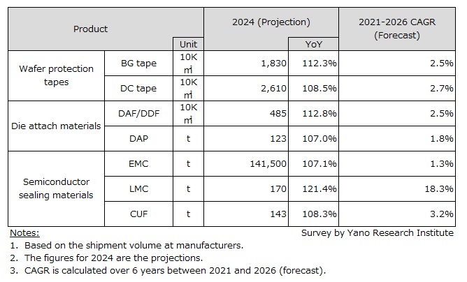
Global semiconductor fabrication process materials and sub-materials market on 7 items of for 2024 are forecasted as follows: BG tape – 18.3 million㎡ (112.3% YoY), DC tape – 26.1 million㎡(108.5% YoY), DAF/DDF – 4.85 million㎡(112.8% YoY), DAP – 123 t(107.0% YoY), EMC - 141,500 t(107.1% YoY), LMC – 170 t(121.4% YoY)and CUF – 143t(108.3% YoY). The numbers are calculated based on the shipment volume at manufacturers.
Since the outbreak of the novel coronavirus in 2020, telework and online classes became the norm, significantly boosting demand for smartphones and PCs. At the same time, data transmission volumes surged, driving major investments in data centers and other infrastructure. As a result, the demand for semiconductors grew at an accelerated pace.
Starting in 2022, however, as pandemic-related restrictions eased and economic activities picked up, consumer spending on entertainment (such as dining out, travel, and leisure) began to recover. As a result, the surge in demand for IT equipment tied to telework slowed. This shift led to a sharp decline in demand for digital devices, which in turn caused semiconductor demand to stagnate.
Due to its close alignment with semiconductor demand, the global market for semiconductor fabrication materials and sub-materials hit rock bottom in 2023. However, since then, it has shown signs of recovery. We expect the market to fully emerge from this downturn in 2024, with many categories projected to experience positive growth of 3 to 8% starting in 2025.
Noteworthy Topics
Sealing Materials for Advanced Packaging Applications
Transfer molding with epoxy molding compounds (EMC) is the most widely used method for encapsulation in the semiconductor industry.
Meanwhile, in advanced packaging applications like Fan-Out Wafer-Level Packaging (FO-WLP) and Panel-Level Packaging (PLP), Liquid Molding Compound (LMC) is gaining traction. LMC offers superior flowability, making it ideal for large surface areas and thin-film molding. It also excels in void control, outperforming granules in suppressing void formation, and is dust-free, making it well-suited for clean room environments.
Package warpage has been a common issue with LMCs. To address this, some manufacturers have developed granular materials for EMCs to reduce the tendency for narrow gap filling and warping. Granular encapsulating compounds are now being used in advanced packaging through compression molding.
Compression molding involves supplying liquid or granular resin into a heated mold cavity, where it is then compressed into the desired shape. This method offers several advantages, including higher resin efficiency and the elimination of runners or gates, which are typically seen in transfer molding.
Compression molding helps reduce material costs by minimizing resin flow during the molding process. This reduces the impact on chips and wires, improving the moldability of packaged products and enabling thinner wires. Additionally, by using the face-down method, which ensures uniform resin distribution, compression molding allows for consistent and ultra-thin molding. This approach is particularly well-suited for large-size FO-WLP/PLP applications.
In advanced packaging technology, the development and introduction of sheet epoxy encapsulants are underway. These encapsulants allow for large-area bulk encapsulation and address flow marks (appearance defects), which have been a challenge with LMC. However, LMC remains the dominant choice for now, as switching to the sheet epoxy encapsulant method requires companies to replace existing equipment at their production facilities.
Future Outlook
In advanced stacking technology for High Bandwidth Memory (HBM) products, the TC-NCF method is set to become the industry standard. This process involves bonding chips together using heat and pressure (Thermo-Compression) after applying a Non-Conductive Film (NCF) between the layers.
To meet the rapidly evolving demands for memory products—such as smaller size, higher speed, and greater bandwidth—SK Hynix (Korea) introduced its proprietary process, MR-MUF (Mass Reflow Molded Underfill), using LCMUF (Liquid Compression Mold Underfill) for HBM3 and subsequent products. This innovation has allowed SK Hynix to significantly outpace Samsung Electronics.
By achieving a breakthrough in thermal control with MR-MUF, SK Hynix has solidified its leadership in the HBM market. In a broader sense, it can be said that semiconductor materials have played a key role in reinforcing SK Hynix’s competitive edge.
For stacking technology in HBMs with 16 or more layers, both the TC-NCF and MR-MUF methods are approaching their limits in terms of bump pitch. Hybrid Copper Bonding (HCB), using Cu-Cu bonding, is gaining attention as the preferred technology for producing 16-layer or higher HBMs.
SK Hynix has announced that it is considering both Advanced MR-MUF and HCB for its next-generation HBM stacking process. However, since HCB is still in development, it may not be ready by their target year of 2026. It's important to note that if the HCB method is successfully established, materials like NCF and LCMUF may become obsolete.
This shift presents a significant opportunity for semiconductor material manufacturers to enter the market and drive competition in emerging areas. The semiconductor company that can anticipate the industry's future needs and develop the necessary materials will be well-positioned to dominate the next-generation semiconductor materials market.
Research Outline
2.Research Object: Manufacturers of wafer protection tapes, die attach materials, and semiconductor sealing materials
3.Research Methogology: Face-to-face interviews by our expert researchers (including online interviews) and literature research
What is the Semiconductor Fabrication Process Materials and Sub-Materials Market?
In this market research, the semiconductor fabrication process materials and sub-materials market targets back grind tape (BG tape), dicing tape (DC tape), die attach film (DAF)/dicing die attach film (DDF), die attach paste (DAP), epoxy molding compound (EMC), liquid molding compound (LMC), and capillary underfill (CUF). The market size is calculated based on the shipment volume of manufacturers.
<Products and Services in the Market>
BG tape, DC tape, DAF/DDF, DAP, EMC, LMC, CUF
Published Report
Contact Us
The copyright and all other rights pertaining to this report belong to Yano Research Institute.
Please contact our PR team when quoting the report contents for the purpose other than media coverage.
Depending on the purpose of using our report, we may ask you to present your sentences for confirmation beforehand.