No.3790
Global Semiconductor Packaging Substrate Materials Market: Key Research Findings 2025
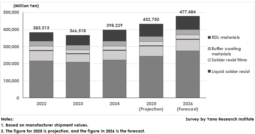
Global Shipment Value of Semiconductor Packaging Substrate Materials Is Projected to Reach \432.750 Billion, an 8.7% Increase YoY
Yano Research Institute (the President, Takashi Mizukoshi) surveyed the global market for semiconductor packaging substrate materials and found out the trends by product segment, trends of market players, and the future outlook.
Market Overview
Based on manufacturer shipment values, the global market size for semiconductor packaging substrate materials was 398.229 billion yen, marking an 8.7% year-over-year increase. By segment, the values were as follows: copper clad laminates (CCL) reached 222.423 billion yen, build-up films 54.250 billion yen, liquid solder resist 3.650 billion yen, solder resist films 21.650 billion yen, buffer coating materials 28.851 billion yen, and redistribution layer (RDL) materials 67.450 billion yen.
Demand for semiconductors surged after the outbreak of the novel coronavirus in 2020 due to increased demand for IT devices, including PCs and smartphones, for remote work and online classes, as well as a series of large-scale investments in data centers stemming from tremendous increases in data traffic caused by the promotion of teleworking.
However, demand for IT-related devices has expired since around 2022, as economic activities that were restricted during the pandemic crisis have resumed, reviving the service industries, such as food services, travel and entertainment, and reorganizing the environment for online meetings, etc. This has caused IT-related products to rapidly become sluggish, which reduced semiconductor demand.
The market for packaging substrate materials tends to align with these trends. Consequently, the market decreased to 366.180 million yen in 2023, which is 95.6% of the size of the previous year.
Despite the delayed recovery of semiconductors for memory or automobiles, the following factors upturned the market in 2024: higher unit prices for CCLs stemming from thicker core films in Flip Chip-Ball Grid Array (FC-BGA) substrates to prevent warpage as packaging materials grow larger; an increased variety of materials for FC-BGA substrates due to increased demand for AI accelerators, such as GPUs and ASICs; and the growing use of RDL materials in cutting-edge packages that require multilayer forming. The global market for semiconductor packaging substrate materials is expected to continue growing at a rate of around 8 to 10% in 2025 and beyond.
Noteworthy Topics
Material Development Is Underway With Anticipated Changes to Package Designs
Glass core substrates and co-packaged optics (CPOs) are expected to become promising next-generation packaging substrates.
In recent years, dramatic improvement is required in the performance and quality of packaging substrates as semiconductor device performance and density have become increasingly high. Since conventional substrates based on organic materials are considered difficult to meet the required specifications from the aspects of coefficient of thermal expansion, rigidity, and heat dissipation performance, glass core substrates are regarded as the alternative. Nevertheless, glass core substrates have disadvantages of difficulty in processing and higher prices than organic core substrates, so that their applications are likely to be limited, such as for semiconductor packaging substrates for AI. Since glass core substrates excel in size stability, low thermal expansion, rigidity, high resilient rate, and substrate surface smoothness, they are expected to achieve further higher performance and density.
However, due to their different material characteristics compared to organic core substrates, glass core substrates may crack during dicing, drilling, or handling processes. The demand for specifications different from those of organic core substrates presents an opportunity for material manufacturers to develop new materials and to enter the market.
Future Outlook
Over time, glass core substrates will likely prevail as technological reforms solve the current challenges of high cost and processing difficulties. This is evident in the production of larger LCD panels, which used to be considered impossible but are now commonplace. It is too late for material manufacturers to prepare for technologies after they have become newsworthy. Continued technological development that anticipates the future changes is the source of the Japanese companies’ current competitive edge.
Currently, Japanese manufacturers dominate the market for semiconductor packaging substrate materials. To maintain this position with the next-generation packaging substrates and become a major supplier in the ever-changing semiconductor industry, it is necessary to understand market changes and align them with technological development in order to respond to customer needs.
However, there is no guarantee that the supply chain for cutting-edge semiconductors will remain the same. To secure a position in the supply chain, it is important to identify new features and product requirements, as well as changes in demand. It is also important to continue developing technologies that fulfill these requirements.
Material manufacturers who are not currently in the supply chain or who have not secured a certain market share can gain a competitive edge in next-generation technologies by identifying the need for the next cutting-edge materials and by providing them to semiconductor manufacturers in a timely manner.
Research Outline
2.Research Object: Copper‐clad laminate (CCL) manufacturers, build-up film manufacturers, solder resist manufacturers, buffer coating material manufacturers, redistribution layer (RDL) material manufacturers
3.Research Methogology: Face-to-face interviews by expert researchers (including online), and literature research
Global Semiconductor Packaging Substrate Material Market
This research focuses on the global market for semiconductor packaging substrate materials, particularly on copper clad laminates (CCLs), build up films, liquid solder resists, solder resist films, buffer coating materials, and redistribution layers (RDLs). The market size was calculated based on manufacturer shipment values.
<Products and Services in the Market>
Copper clad laminates (CCLs), build up films, liquid solder resists, solder resist films, buffer coating materials, and redistribution layer (RDL) materials.
Published Report
Contact Us
The copyright and all other rights pertaining to this report belong to Yano Research Institute.
Please contact our PR team when quoting the report contents for the purpose other than media coverage.
Depending on the purpose of using our report, we may ask you to present your sentences for confirmation beforehand.